
PCB design services
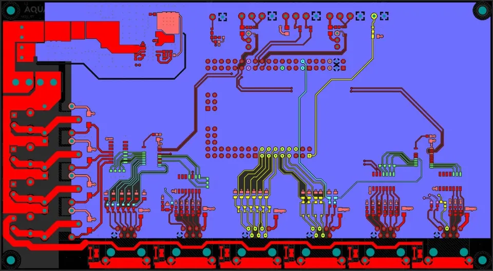
Our PCB design services take a circuit from schematic to a board that can be built, tested and certified. We design 2 to 6 layer boards for industrial controllers, power electronics, EV chargers and connected devices, and we hand over every source file, so the design stays yours to change and manufacture.
Where we start from
We can work from what you have:
A schematic from another tool that needs review before layout
A block diagram, a datasheet reference design or a hand sketch
A description of what the board must do, if you also need the circuit designed
When the circuit is not yet designed, the work begins with our electronic device design service, and the PCB layout follows from it.
How the work is done
Schematic and component choice
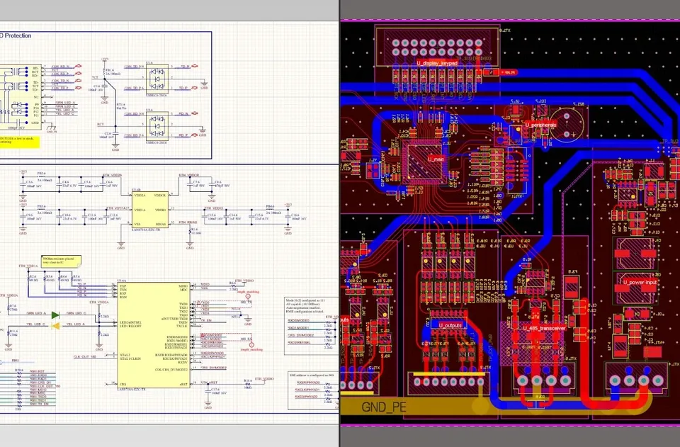
We capture or review the schematic and choose each part for availability, lifetime and price, with an alternative for every part that has one. Footprints and symbols are built or checked against the manufacturer's drawings. Inputs, outputs and pins are mapped with the firmware engineer, so the layout matches how the software will use the board.
Stack-up and placement
We choose the layer count and stack-up with the fabricator in mind, and place parts by function: power, analog, digital and high-voltage areas kept apart, connectors where the enclosure needs them. For multilayer PCB design we plan reference planes, controlled impedance where the signals need it, and the return path of every fast signal.
Routing
Power paths are sized for their current and temperature rise. Sensitive analog signals are routed away from switching nodes. Creepage and clearance distances are set for the working voltage and the safety standard the product falls under.
Design for manufacture and test
Before release, every board is checked against the fabricator's and the assembler's rules: copper and drill limits, solder mask and paste layers, fiducials, panel layout, test points and polarity marks. Boards meant for automated assembly are prepared for it from the start, so a prototype and a production board are the same design.
Review with you
You review the schematic and the layout before release, with 3D views of the assembled board. We check the fit in the enclosure with the mechanical model before any board is ordered.
What you receive
Schematic as PDF and as source files
PCB layout source files
Gerber, drill and pick-and-place files
Bill of materials with manufacturer part numbers and alternatives
Assembly drawing and 3D model of the assembled board (STEP)
Fabrication notes: stack-up, materials, finish and tolerances
On request, a test plan and test-point list for functional testing
Custom PCB design for real conditions
Most of the boards we lay out run in cabinets, chargers and machines, not on a desk. That means mains voltages next to low-voltage logic, relays and contactors switching inductive loads, long cables carrying RS-485 or CAN, and enclosures without airflow. A custom PCB design for these conditions is mostly about what is kept apart and how heat leaves the board, and it is checked again during compliance testing.
Tools
We design in Altium Designer and can deliver in KiCad. Mechanical fit is checked in SolidWorks, and circuits are simulated in LTspice where the design calls for it. An Altium PCB design comes with its full project, libraries included.
PCB layout services on their own
If your team designs the circuit and only needs the layout, we work from your schematic and your rules, and deliver in your tool's format where we can. We can also review a layout you have already made, before it is sent for manufacture.
After the layout
Boards can be assembled in our workshop as prototypes or pilot units, see SMT assembly, or released to a partner factory for a larger run. Either way, the first boards are brought up and tested before the design is called finished.